

01.What is a Via Stub?
Standard Plated Through Holes (PTH) in multilayer boards penetrate the entire board. However, most high-speed signals only need to connect a few specific layers. The unused, floating copper barrel segments remaining in the hole are known as Via Stubs.
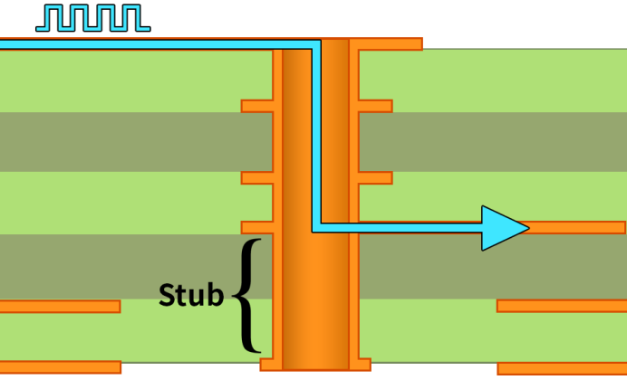
Essentially, a via stub acts as an unterminated microstrip stub. It forms a λ/4 resonator with the main signal, reflecting energy like an "echo chamber." The longer the stub, the lower its resonant frequency.
Based on the quarter-wavelength resonance formula, when the signal frequency f satisfies f = c / (4 × L × √Dk) (where c is the speed of light, L is the stub length, and Dk is the dielectric constant of the substrate), total reflection occurs at the end of the stub. At this point, the stub reaches exactly a quarter of its effective wavelength. The superposition of the reflected and incident signals creates a parallel resonance, causing a sharp drop in impedance, severe signal reflection, degraded return loss, and worsened insertion loss spikes.
Taking FR-4 (Dk = 4.0 @ 10GHz) as an example: a 10-mil stub resonates at approximately 11.8 GHz, while a 5-mil stub shifts the resonance up to about 23.6 GHz. In practice, a single 8-mil PTH stub can cause a resonance dip exceeding -15 dB at 12.5 GHz.
During actual design, you can use the formula above to calculate the resonant frequency caused by the stub. If this frequency falls within the signal's operating band, the stub must be mitigated. For low-speed, thin, or standard boards where stub effects are negligible, the extra cost of backdrilling can be avoided.
02. What is Backdrilling?
Backdrilling, also known as Controlled Depth Drilling (CDD), involves using a drill bit larger than the original Plated Through Hole (PTH) to drill from the back of the board, effectively removing the excess copper via stub to improve Signal Integrity (SI).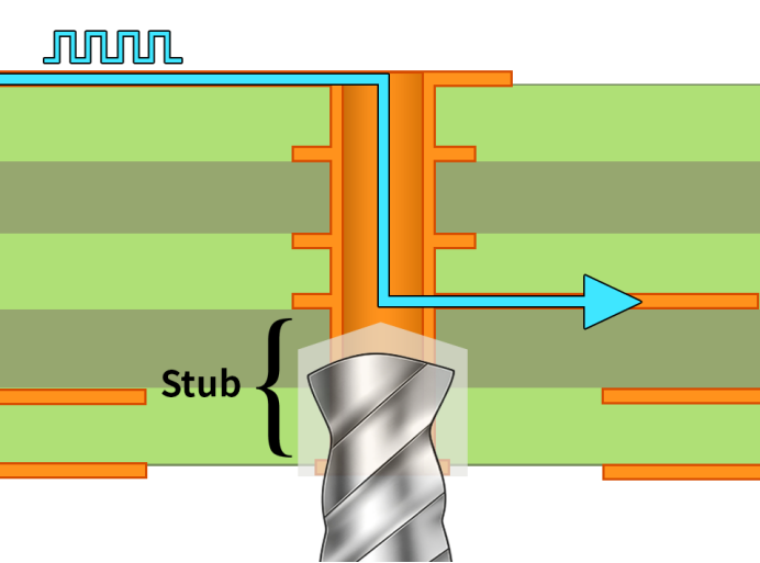
Before backdrilling, standard through-hole drilling, desmearing, and plating must be completed to generate a fully plated through-hole.
For Stub ≤ 10 mil: A CCD drill with a larger drill bit is used to drill from the back (stub side) with precise depth control, removing the stub while strictly maintaining tolerances to prevent damage to the active signal layers.
For Stub ≤ 8 mil: 3D Backdrill + Advanced Mapping processes are required. The typical workflow includes: drilling and plating standard vias, X-ray CT 3D scanning to locate signal layers, Advanced Mapping alignment algorithms to calculate the individual Z-axis stop-drill depth for each backdrill hole, 3D Backdrill execution to the target depth, plasma cleaning to remove hole wall debris, CT scanning, and automatic measurement of the actual stub length for each hole. Finally, Backdrill AOI is used to detect missed drills, drill deviation, and plugged holes.
03. Backdrilling Design Guidelines
During the PCB design phase, Design for Manufacturability (DFM) rules for backdrilling must be strictly followed to ensure the design stays within the supplier's manufacturing capabilities.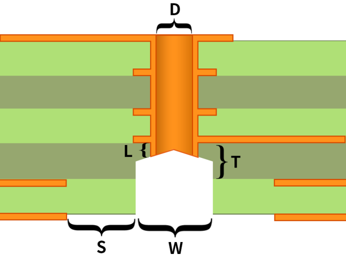
D (Via Hole Diameter): 0.2–0.5 mm. After backdrilling, all finished through-holes must be resin-plugged.
W (Backdrill Diameter): Determined by the via size; typically 0.2 mm larger than the via drill size. In dense BGA areas, it can be 0.15 mm larger.
S (Safety Clearance): ≥ 0.15 mm from the backdrill edge to pads, traces, or copper pours. In dense BGA areas, this can be reduced to ≥ 0.125 mm.
T (Dielectric Thickness Between Drilled and Undrilled Layers): ≥ 0.15 mm. Values below this threshold require technical review.
L (Stub Length): Standard backdrilling achieves Stub ≤ 10 mil, while 3D backdrilling can control it to ≤ 6 mil. The more vias requiring backdrilling, and the smaller the allowable stub length, the higher the PCB manufacturing cost