
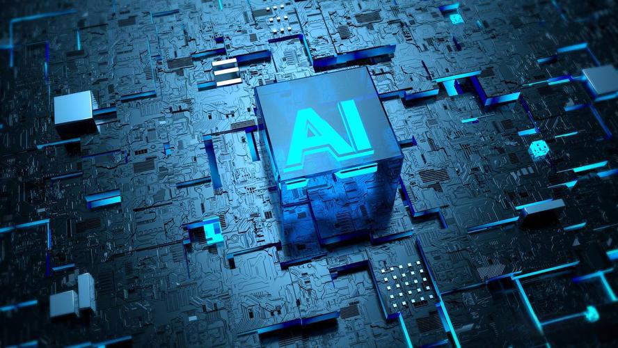
In what aspects can AI assist in PCB design?
AI is reconfiguring the PCB design process from three dimensions: efficiency, quality, and cost, transforming the "experience-driven" approach into a "data-driven" one.
First. Schematic Design Phase: AI helps you "make fewer mistakes and achieve faster matching"
1. Intelligent schematic verification: Automatically detects short circuits, pin floating, signal conflicts, and parameter errors. It is 10 times faster than manual verification.
2. Automatic packaging matching: Match the packaging for each device model with just one click, reducing the possibility of manual input errors.
3. Network Intelligence Optimization: Automatically merge redundant networks and optimize power/ground topologies.
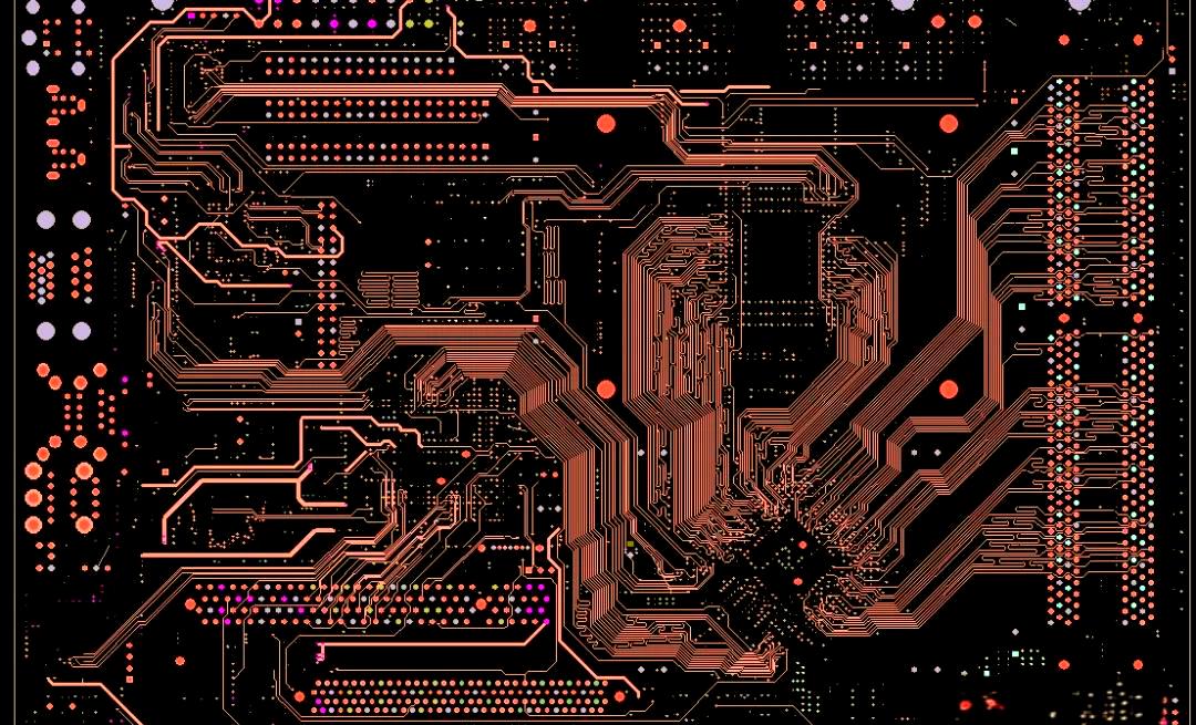
Second.Layout and Wiring (Core Breakthrough): AI acts as a "Super Layout Engineer"
1.Intelligent automatic layout
Arrange them automatically by electrical, heat dissipation, EMI and structural categories (for example, heat-generating components placed at the sides, sensitive components kept away from interference);
High-speed/radio frequency/power isolation, automatic alignment of interfaces, optimized BGA fan-out;
Output 3 to 5 sets of solutions for selection, while retaining the manual control rights.
2. AI Intelligent Wiring (Improvement in both speed and quality)
• Standard 4-layer board: Completed in 2 hours (compared to 3 days in the traditional method).
• High-speed signals: Automatic differential pair, equal-length matching, impedance control, crosstalk suppression.
Real-time SI/PI constraint-driven: Wiring ensures compliance, reducing post-simulation rework.
Automatic optimization of through-hole/drill-through/anti-pad soldering, reducing impedance fluctuations.
3. Representative tools:
Cadence Cerebrus, Zuken CR-8000, JITX, SailWind.
Third. Simulation Verification: AI Transforms "Hourly" to "Minute-level"
• Electromagnetic/thermal/power simulation acceleration: AI replaces part of the computation, resulting in a speed increase of 10 to 100 times.
• Real-time risk prediction: Intercept over 70% of SI/PI/EMC issues in advance.
• PDN/thermal optimization: Automatically optimizes power distribution and via heat dissipation, with ripple ≤ 20mV and thermal resistance reduced by 15%.
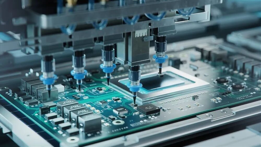
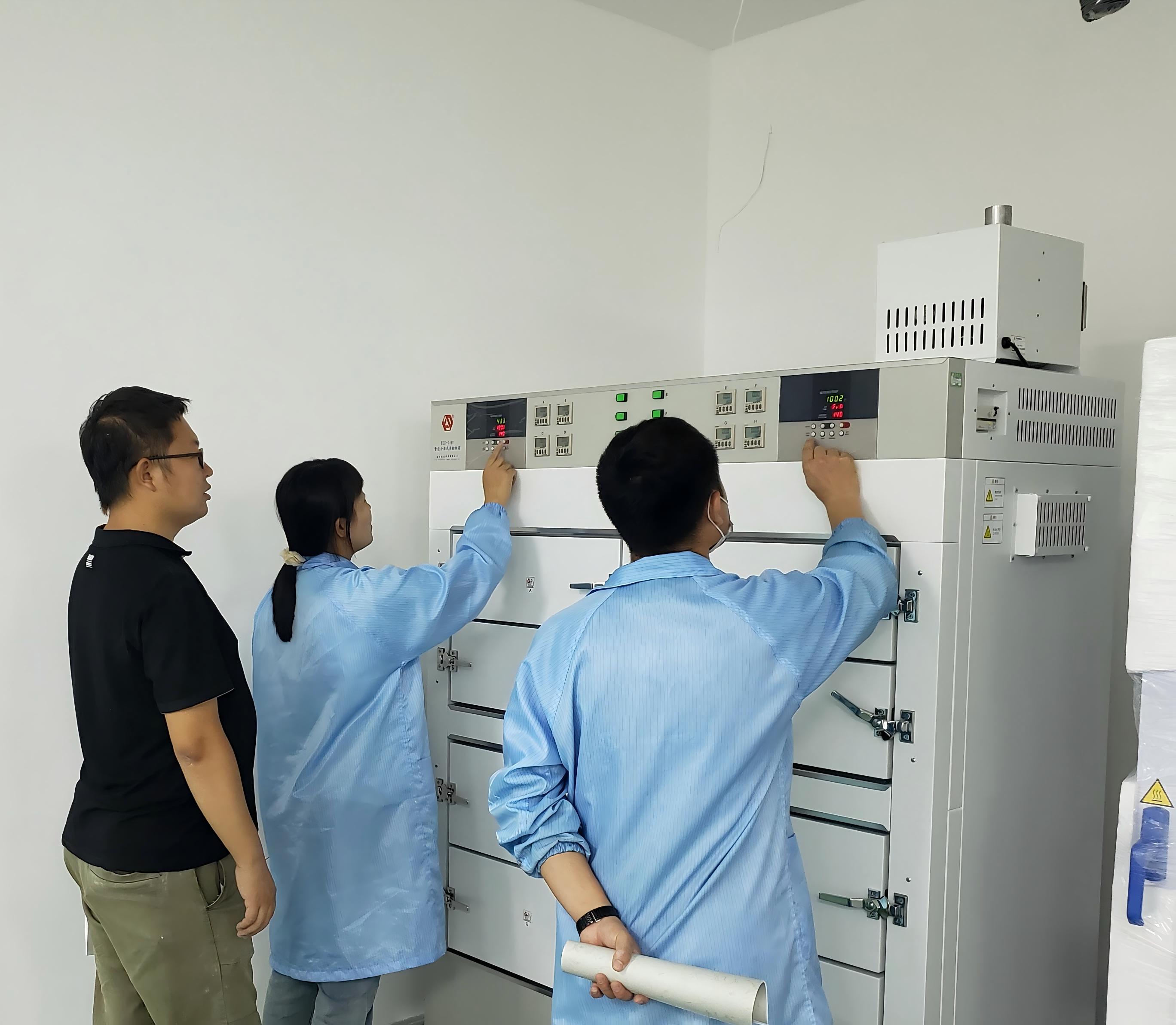
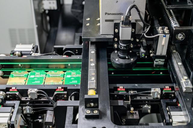
Forth. DFM/DFA Manufacturability: AI Helps You "Succeed in Plating Once"
• Intelligent DRC+ process inspection: Not only checks design rules, but also matches the factory process (line width / spacing / hole diameter / stencil).
• Defect Prediction: By analyzing AOI data, it can alert for risks such as false soldering, copper foil tearing, hole deviation, and short circuits.
The production failure rate has decreased by more than 30%, and the success rate of one-time board placement has reached 95% or higher.
Fifth. Other Key Applications
Reverse engineering: AI scanning + recognition, automatically generating schematic diagrams/netlists, eliminating the need for manual board disassembly.
• HDI/High Density Optimization: Wire density increased by 50%, volume reduced by 40%, suitable for 5G, mobile phones, and automotive electronics.
• Cost/ Material Optimization: Automatically recommends the type of sheet, number of layers, and process, balancing performance and cost.
In summary, AI can shorten the PCB design cycle by 40% - 60%, increase the pass rate to 95% or higher, increase the production yield by 10% - 15%, and significantly reduce labor costs.